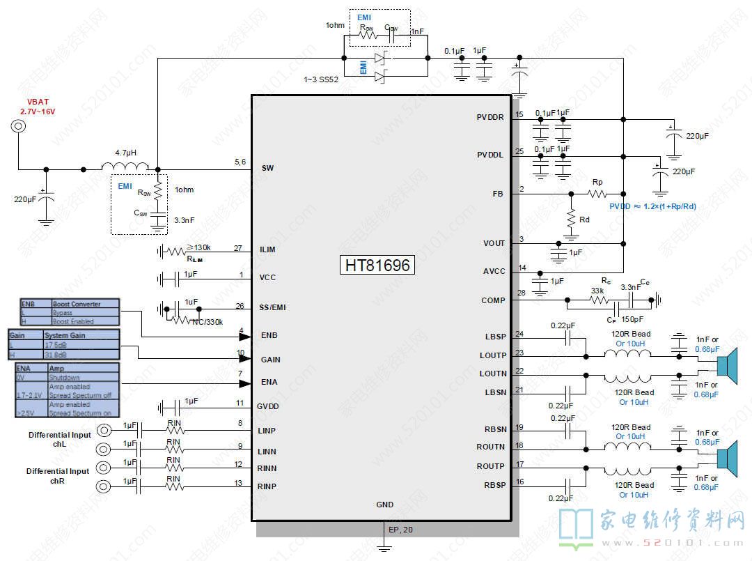
概述:HT81696是一款内置升压的立体声D类音频功率放大器,它支持单节锂电、双节锂电串联、 5V、12V等多种输入,升压后的电压提供给功放供电,功放支持双通道立体声BTL输出以及并联PBTL单声道输出。 HT81696内置的升压电路,可通过FB脚设置升压值,以满足不同的输出功率需求。其还可通 过外置电阻调节开关峰值电流限值。 此外,HT81696内部集成免滤波器调制技术,能够直接驱动扬声器,内置的关断功能使待机电流最小化,还集成了输出端过流保护、片内过温保护、输入电源欠压异常保护、升压电压过压保护等功能。
一、HT81696功能和特性
・输出功率(fIN=1kHz, RL=4Ω, BTL)
双锂电8.4V:2×30W (VOUT=16V, THD+N= 10%)
单锂电3.7V:2×10W (VOUT=9V, THD+N = 10%)
・输出功率(fIN=1kHz, RL=3Ω, PBTL)
双锂电7.2V:52W (VOUT=17V, THD+N= 10%)
单锂电3.7V:15W (VOUT=9V, THD+N = 10%)
・输出功率(fIN=1kHz, RL=4Ω, PBTL)
单锂电3.7V:20W (VOUT=12V, THD+N = 10%)
・VBAT供电范围:2.7V至VOUT
・D类功放扩频功能
・内置升压电路:可调节的升压值和升压限流
・保护功能:过流/过热/欠压异常/过压保护功能
・无铅无卤封装,ETSSOP28
二、HT81696引脚功能

| 管脚号 | 引脚功能 | I/O | 引脚说明 |
| EP | GND | G | Ground. Also provides thermal connection from the device to the board. A matching ground pad should be provided on the PCB and the device connected to it via solder. 地,同时提供器件向板级散热的路径。PCB板上需要留有足够的铺地露铜与之良好焊接。 |
| 1 | VCC | O | Output of the internal regulator for boost converter. A ceramic capacitor of 1uF isrequired between this pin and ground. 升压电路内部电压输出,接1uF到底。 |
| 2 | FB | I | Voltage feedback. 电压反馈脚 |
| 3 | VOUT | P | Power supply for boost converter. 升压供电端 |
| 4 | ENB | I | Enable logic input for boost converter. Logic high level enables the device. Logiclow level disables the device and turns it into bypass mode. 升压使能脚,高电平时升压开启,低电平时升压关闭 |
| 5,6 | SW | P | The switching node pin of the converter. 升压开关点 |
| 7 | ENA | I | Enable logic input and operation mode selection for amplifier |
| 8 | LINP | I | Positive input (differential+) for audio amplifier of left channel. 音频左声道输入正端。 |
| 9 | LINN | I | Negative input (differential-) for audio amplifier of left channel. 音频左声道输入负端。 |
| 10 | GAIN | I | Gain select pin. Gain is 17.5dB when logic low, and 31.8dB when logic high orfloating 增益选择。拉低时,增益17.5dB;拉高或悬空时,增益31.8dB |
| 11 | GVDD | O | Voltage regulator of amplifier, connect 1uF to GND. 功放内部电压,接1uF到地 |
| 12 | RINN | I | Negative input (differential-) for audio amplifier of right channel. 音频右声道输入负端。 |
| 13 | RINP | I | Positive input (differential+) for audio amplifier of right channel. 音频右声道输入正端 |
| 14 | AVCC | P | Analog power supply for amplifier 功放模拟供电 |
| 15 | PVDDR | O | Power supply terminal for right channel. 右声道功率电源端。 |
| 16 | RBSP | BST | Connection point for the ROUTP bootstrap capacitor, which is used to create a powersupply for the high-side gate drive for ROUTP. ROUTP自举电容端 |
| 17 | ROUTP | O | Positive output terminal (BTL+) for right channel. 右声道正端输出 |
| 18 | ROUTN | O | Negative output terminal (BTL-) for right channel. 右声道负端输出。 |
| 19 | RBSN | BST | Connection point for the ROUTN bootstrap capacitor, which is used to create apower supply for the high-side gate drive for ROUTN. ROUTN自举电容端 |
| 20 | PGND | P | Power ground for amplifier 功放功率地 |
| 21 | LBSN | BST | Connection point for the LOUTN bootstrap capacitor, which is used to create a powersupply for the high-side gate drive for LOUTN. LOUTN自举电容端 |
| 22 | LOUTN | O | Negative output terminal (BTL-) for left channel. 左声道负端输出。 |
| 23 | LOUTP | O | Positive output terminal (BTL+) for left channel. 左声道正端输出。 |
| 24 | LBSP | BST | Connection point for the LOUTP bootstrap capacitor, which is used to create a powersupply for the high-side gate drive for LOUTP. LOUTP自举电容端 |
| 25 | PVDDL | P | Power supply terminal for left channel. 左声道功率电源端。 |
| 26 | SS | O | Soft-start programming pin. An external capacitor connected to ground sets the ramprate of the internal error amplifier’s reference voltage during soft-start. 升压软启动设置脚,接电容到地。 Also used as mode selection for different tr/tf, an external resistor connected toground selects a flatter tr/tf. 同时作为tr/tf设置脚,当同时外接1个330k电阻到地时,选择较缓的tr/tf。 |
| 27 | ILIM | I | Adjustable switch peak current limit. An external resistor should be connectedbetween this pin and GND. 最大限流值设置端,外部接电阻到地。 |
| 28 | COMP | O | Output of the internal error amplifier, the loop compensation network should beconnected between this pin and the AGND pin. 内部补偿脚 |
三、HT81696典型应用电路
网友评论